Assembling the PC Board
From Spare Time Gizmos' Wiki
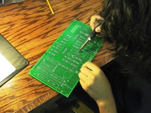
Because the SBC6120-RC fits everything onto a single PC board, it has parts mounted to both sides of the PCB. Begin assembly of your SBC6120-RC by soldering most of the components on the back side of the PC board. Don't be tempted to skip ahead and solder the front side parts such as the switches and LEDs! You won't be able to solder some of the back side parts and you won't be able to fit the faceplate properly if you do.
- Verify all the parts against the packing list.
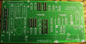
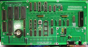
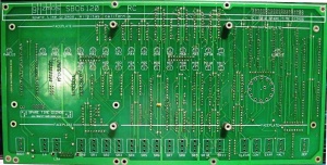
- Identify the front and back of the circuit board. The front has a small silkscreened label on the left side that reads, “LEDS & SWITCHES THIS SIDE.” The front also has the silk screen for the LEDs, the switches, the register display rotary selector switch, and the "|g|i|z|m|o|s| SBC6120-RC" logo . The rear of the circuit board is characterized by the label, “COMPONENTS THIS SIDE,” near the right edge of the board as well as the outlines of all the integrated circuits, the VT6 mounting area, and several of the Spare Time Gizmos "glider" logos.
- Most of the components will be mounted on the rear of the circuit board and soldered on the front. The LEDs, front panel switches, and the register display rotary selector switch will be mounted on the front and soldered on the rear.
- The first component to be mounted will be mounted on the front (switch and LED) side of the board. Locate the small silk-screen rectangle approximately mid way between LED MD6 and switch SR6. Install a .01μF bypass capacitor (marked 103). Solder on the back side of the board. Be sure that the leads appear in the center of the outline of U1. Clip the leads flush with the surface of the board as the socket for U1 will be installed over this point in the next step.
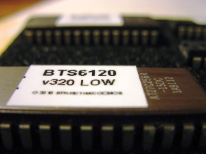
- Mount the integrated circuit (IC) sockets first. If you bought the kit of parts, then sockets are supplied for the CPU (U1), EPROMs (U6 and U7) and GALs (U4, U13, U14, U31). The EPROMs and GALs are programmable and the sockets allow for future modifications to the code. If you wish, you may add sockets for the other ICs as well. If you do, be sure to use good quality machined-pin IC sockets. These are more expensive but will make good contact with the chip pins even after many years. They will also survive more insertion and removal cycles.
- Pin-1 for an IC is indicated by a square pad. This is also true for the SIP (single in-line package) resistor packs. In addition, the silk-screen outlines for the ICs have a V-shaped notch at one end. That denotes the notch or the pin-1 end of the IC. The chip socket should also have a notch or other notable indentation/marking. Be sure that it coincides with the V-shaped mark on the IC outline on the board.
- When soldering sockets or chips to the board solder only two pins, one on each end of the socket or IC at first. If you find that the IC or socket is not laying flat against the board you can reheat the soldered pin and press the IC or socket flat against the board. Once you have done that solder all the rest of the pins on the socket or IC.
□ - U1 socket (HD6120)
□ - U6 socket (PROM high)
□ - U7 socket (PROM low)
□ - U13 socket (IOT1)
□ - U14 socket (IOT2)
□ - U4 socket (MEM1)
□ - U31 socket (MEM2)
- Install all other sockets you intend to install.
- Install the remaining twenty nine 0.01μF bypass capacitors (marked 103). They are mounted at the pin-1 (notch) end of each IC position and one at the top of the crystal oscillator OSC1. U1, the CPU has one at each end (as well as the one in the middle already installed in step 3). They go in the small rounded-end silk-screen outline. Note that ICs U10 and U11 are not supplied with the kit (these are extra SRAMs to expand the memory size) and no bypass should be installed there. If you elect to add these two parts yourself, be sure to add two additional bypass capacitors as well.
- Install the remaining ceramic monolithic capacitors, C12 and C13.
□ - C12, 68pF (680) below OSC1
□ - C13, 68pF (680) below OSC1
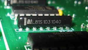
- Now install the resistor packs. The resistor packs (SIPs) mount into a single row of holes labeled 'RPx', where 'x' is the pack number, e.g. RP1. At one end of the resistor pack mounting is a pad with a square outline. This denotes pin 1. When you mount the resistor pack ensure that the end of the resistor pack with the dot or the '1' is mounted to the pad with the square outline. Solder only one pin. Verify that the resistor pack is flush with the board. If not, reheat the solder and push the pack flush with the board. Reverify pin 1 of the pack is in the pad with the square outline. Solder the rest of the pins. Be sure not to confuse the 560 ohm packs with the 10K packs - the 560 ohm ones will be marked "561" and 10K will be marked "103". Use an ohm meter to verify if you have any doubts.
□ - RP1, 10-pin 560Ω (above U26)
□ - RP2, 10-pin 560Ω (above OSC1)
□ - RP3, 8-pin 560Ω (above U26)
□ - RP4, 8-pin 560Ω (above OSC1)
□ - RP7, 10-pin 10K (below U12)
□ - RP10, 10-pin 10K (below U11)
□ - RP5, 8-pin 10K (below U21)
□ - RP6, 8-pin 10K (below U3)
□ - RP9, 8-pin 10K (between U13 and U14)
□ - RP11, 8-pin 10K (between U27 and U25)
□ - RP12, 8-pin 10K (between U25 and U26)
□ - RP8, 6-pin 10K (below U3)
- Install the resistors on the board.
□ - R1, 10K (brown, black, orange) (near U32)
□ - R2, 18K (brown, grey, orange) (near U32)
- If you will be installing the VT6 daughter card, install R6, 10K (brown, black, orange) below D2. Otherwise leave this location open.
- R3, R4 and R5 are not used and nothing should be installed in those locations.
- There is one diode (three if you have the VT6) on the board. Unlike the ceramic capacitors and the resistors, diodes are polarized and must be installed in the correct direction. The cathode end of the diode is signified by a band. Be sure to properly orient the diode before soldering.
□ - D1, 1N6267, large epoxy package, band up, above J3
- If you will be installing the VT6, also install
□ - D2, 1N4148, small glass package, band toward U21
□ - D3, 1N4148, small glass package, band toward U21
- If you will not be installing the VT6, install a jumper in place of D2. Use the clipped-off leads from a resistor or capacitor to make a U-shaped jumper to fit into the holes.
- It is now time to solder in the ICs that will be soldered to the board. These instructions assume you will be soldering the ICs with the exception of the CPU (U1), the EPROMs (U6, U7), and the GALs (U4, U31, U13, U14). ICs ARE STATIC SENSITIVE! Be sure you, your soldering iron, your work area, and you are properly grounded. You don't want static electricity to destroy an expensive and irreplaceable IC like the HD6120 CPU.
- To mount each IC in a socket or to make it fit within the holes on the board, you may need to bend the leads of the IC inward slightly. Place the IC on its side and press down gently but firmly to bend the leads inward. Repeat on the other side until all the leads will fit within the pins of the socket or in the holes on the board. Remember, pin-1 of the IC goes to the pad with the square outline, usually the upper-left side of the IC location. If you are soldering the ICs in place, use the same technique used with the IC sockets. Solder two pins at opposite ends of the IC. If the IC is not flush with the board, reheat each soldered pin in turn and press the IC flush with the board. Solder the rest of the pins. Note: If you have installed sockets, use this section to install the ICs in their respective sockets rather than soldering them in.
□ - U12, DS1321
□ - U2, 74HC373
□ - U3, 74HC373
□ - U24, 74HC373
□ - U23, 74HC373
□ - U33, 74HC74
□ - U20, 74HC74
□ - U32, 7555
□ - U27, 74HC366/74HC368
□ - U25, 74HC174
□ - U26, 74HC174
□ - U22, 74HC4040
□ - U16, 74HC174
□ - U30, 74HC366/74HC368
□ - U29, 74HC366/74HC368
□ - U28, 74HC366/74HC368
□ - U21, MAX232
□ - U19, HD6402 UART
□ - U8, 628512 SRAM
□ - U9, 628512 SRAM
□ - U10, 628512 SRAM
□ - U11, 628512 SRAM
- Solder the 4.9152 MHz crystal oscillator to the board. Be sure pin 1 goes to the square pad.
- Install the pico fuse. The pico fuse looks like a small, green resistor and is used to protect the board from damage from either over-voltage or reverse voltage. Should either over-voltage or reverse voltage be applied to the board, D1 will conduct and blow the pico fuse, F1. Install F1 just like installing a resistor.
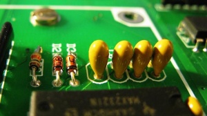
- We will now install the polarized tantalum capacitors. These are egg-shaped and will have a small plus sign '+' near the positive terminal. The silk-screen on the board will have a small '+' near one of the pads. Also, the positive pad on the board has a square outline.
□ - C5, 1μF tantalum capacitor, next to U21, positive lead away from U21
□ - C6, 1μF tantalum capacitor, next to U21, positive lead away from U21
□ - C7, 1μF tantalum capacitor, next to U21, positive lead away from U21
□ - C8, 1μF tantalum capacitor, next to U21, positive lead away from U21
□ - C9, 1μF tantalum capacitor, next to U32, positive lead down (near R2)
□ - C11, 47μF tantalum capacitor, next to D1, positive lead up (connected to banded end of D1)
- Install the battery holder for the lithium coil cell at B1.
- Install the 2x4 pin jumper header for baud rate selection. Locate the silk-screen box labeled BAUD just below U22. Solder one pin and make sure the header is flush to the board before soldering the other pins.
- Install the coaxial power jack. Solder one pin, make sure it is flush, and solder the other pins.
- Install J3, the console RS-232 jack. Snap the jack in place and make sure it is flush with the board. Solder all the pins.
- J2 and J4 are installed only if you have the VT6 terminal module. If you are planning to install a VT6 display module on your system, install the 10-pin connector at J2 and the two-pin connector at J4.
□ - J2, 10 pin header
□ - J4, 2 pin header
- J5 is not used and should not be installed.
- At this point all the sockets and passive components have been installed on the back side of the board. One capacitor should be installed on the front side of the board. Take time to inspect all solder joints. Look for cold joints (grey, grainy connections) and solder bridges (solder that connects to an adjacent pin that shouldn't).
- Do a continuity check using an ohmmeter. Place the positive lead of the ohmmeter on the banded end of D1. Place the negative lead of the ohmmeter on the unbanded end of D1. The resistance reading should rise to a relatively high value, over 1K ohms. If it does not it indicates a reversed component or a short on the board. In that case reinspect your soldering and parts placement.
When you have finished these steps, continue with Assembling the Faceplate.
